PART16Signal Converter
Experiment Purpose
- 1.Investigate the operation principle of the circuit that converts analog signal to digital signal or digital signal to analog signal through experiment.
- 2.Investigate the operation principle of the circuit that converts frequency change to voltage change or voltage change to frequency change through experiment.
Experiment 1 :Analog to Digital Converter
Theory
There are several ways to convert analog signal to digital signal, but here, the circuit composition, operation principle and characteristic of main three ways will be explained. In AD conversion, it is known that the original signal can be reproduced by executing the sampling over double of the maximum frequency included to the input analog signal(Nyquist theorem). Therefore, the higher the frequency of the signal is, the higher speed of ADC it requests. And, the more the bit of output binary number of ADC is, the higher the resolution of ADC is, and the level of input analog signal is more subdivided and expressed as digital signal.
Parallel Comparison ADC
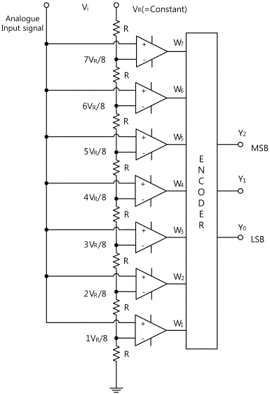
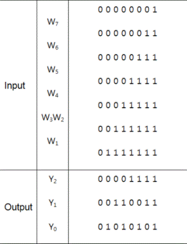
This is a parallel comparison type ADC, also called flash type, and the fastest ADC. Fig.16-2 shows its structure and the level of analog input voltage V1 is compared by parallel comparators and coded as binary number of 3 bit. In this form, to output as n bit, 2n identical resistances and 2n - 1 comparators are needed(For example, with 8 bit ADC, 256 Rs and 255 comparators are needed). According to the level of V1, the lower comparators to which higher "+" terminal voltage is applied all have HIGH output and the outputs of upper comparators all become LOW. For example, when (3/8)VR<V1<(4/8)VR, W1~W3 all become HIGH, and W4~W7 all LOW. In this state, the ADC output becomes Y2Y1Y0=011(=3). Fig.16-3 shows the input/output relationship of encoder. The analog input voltage should not be changed during the conversion, so Sample/Holder circuit should be connected in front of ADC.
The conversion speed is determined by the sum of delays of comparator and encoder, and currently, ADC under 20ns is used. 4~8 bit(16~256 level) is commercialized and if the bit number is bigger than this, the structure gets too big. The number that can be converted in 1 second is called conversion rate, and this is same as the reciprocal of conversion speed.
Dual Slope ADC
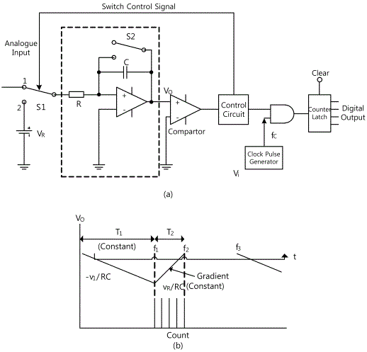
This is suitable for converting precisely the analog signal changing relatively slowly to digital signal. As expressed in fig.16-4, this consists of integrator, comparator and counter. Fundamentally, the clock pulse during the time proportional to the analog voltage is counted and the counted number is outputted as digital signal. The integrator is used to get the time proportional to analog input voltage. In the fig., suppose the standard voltage VR<0, and the analog input voltage Vi>0. At first, the switch S2 is closed(output voltage of integrator V0 = 0) and as S1 is switched as 1 at t=0, S2 is opened. Then, V0 decreases straightforwardly and after T1, V0=-(Vi/RC)T∝Vi, and when t=T1, if S1 is moved to 2, V0 increases with the increase rate of VR/RC. If the time until it becomes V0=0 is called T2, it can be calculated as below.

This circuit is not related to RC so the values of R and C do not have to be precise. If the clock pulse is counted during T2 only with the counter, the number is proportional to Vi and eventually, the digital signal which is proportional to analog input can be earned.
This ADC integrates the analog input voltage and standard voltage twice so it is called dual slope type. From the operation principle, it can be guessed that this circuit is not suitable for high speed ADC. However, the circuit is simple and strong for noise(the noise becomes 0 when integrated. Also, if it is integrated once every 1/60 second, the disturbance of 60Hz is removed), it is frequently used at low speed high precision ADC. For example, this ADC is used for 6 digit(999999 = 106-1 = 221 ; 21 bit) digital voltmeter.
DA Feedback Type ADC
This converts the output digital code of ADC to DA again and compares it to the input signal. There are three types below.
(1) Staircase ADC
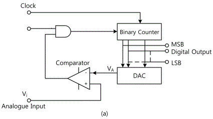
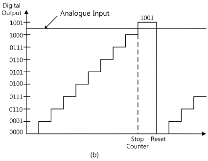
In fig.16-5(a), the analog signal Vi which is S/H-ed is input to “+” terminal of the comparator. When t=0, the binary UP counter is set as 0. Therefore, the output voltage of DAC which is inputted to “-“ terminal of comparator is 0. In fig.16-5(a)., if Vi > VA, the count of the counter becomes UP by 1 following the clock. Therefore, VA increases like staircase as in fig.16-5(b). When VA is over Vi, the code of comparator’s output is changed and the counter is stopped. The result here becomes the digital output. The control circuit resets the counter as 0 and repeats the process above to convert the level of new input signal. This has simple structure but it takes time to get the output(In worst case, 2n-1 clocks are needed; n is the bit number of ADC).
(2) Tracking ADC
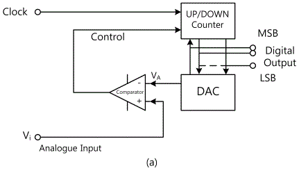
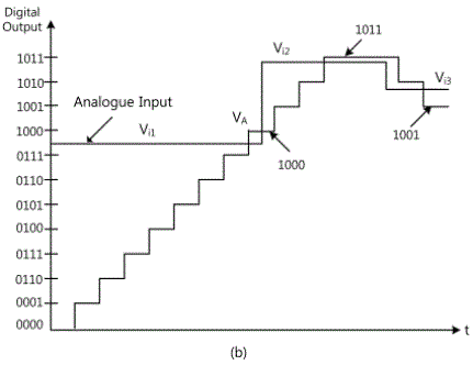
In fig.16-6(a), UP counter of fig.16-5(a) is replaced by UP/DOWN counter and as seen in this fig., it is useful for tracking small changes. Just like the previous case, the counter is set as 0 when t=0. Therefore, DAC’s output voltage VA is "0". When Vi>VA, as the previous case, the count of counter becomes UP by 1 following the clock. <Refer to fig.16-5(b)>. When VA is over Vi, the code of comparator’s output is changed and this time, the counter becomes DOWN by 1. Eventually, the digital output has error as much as ±1LSB from the correct value. As expressed in the fig., the digital output of Vi1=1000, and that of Vi2=1011, and that of Vi3=1001. Like this, it tracks small changes of the input signal.
(3) Successive Approximation ADC
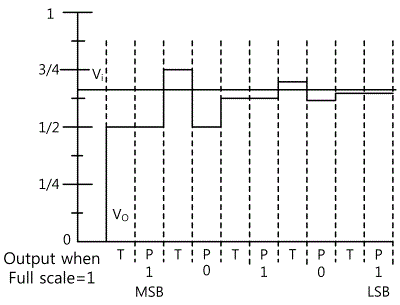
This includes more complex digital circuit instead of the counter. At first, all bits are set as 0. Then, from MSB, each bit should be set as 1 successively. The output of DAC is compared to the input signal Vi at the comparator. If VA is not over Vi, the corresponding bit should be left as 1 and if it is over, the corresponding bit should be set as 0 again. In n bit ADC, complete output bit can be earned by going through this step n times. Let’s find out more specifically with fig.16-7. At first, the comparator compares the input Vi with DAC output VR/2. If Vi>(VR/2), the comparator output is +, and MSB is left as 1, and if Vi<(VR/2), the comparator output is 0, and MSB is set as 0 again. According to MSB being 1 or 0, it becomes (VR/2) + (VR/4) or 0+VR/4. Now, this is compared to Vi, and according to the size, (MSB-1) bit is determined as 1 or 0. This process is repeated n times. Fig.16-7 shows the shape that V0 gets near to Vi gradually. Here, T is test period, and P is the period that the tested and determined bit is sent to the output.
This ADC type is used frequently since its structure is simple and it is relatively precise and fast. Currently, the ADC time of 8~19 bit with this type is 10μs.
Experiment Process
1. Use Circuit-1 of M-16 for the experiment.
2. After connecting between 1e-1f terminal, apply DC 12.75V to 1a-1b terminal.
3.Change R4 and turn on all the LEDs corresponding to Data Output 0~7. Here, adjust the LED corresponding to “0” precisely when it changes from OFF to ON.
4. Check out the status of Date Output LED when the input DC voltage is increased from 0V to 12.75V by 50mV, and record H when ON and L when OFF in the relevant column of table 16-1. Never change R4 here.
tab1Experiment 16-1.1 Analog to Digital Converter Circuit (Compose as Circuit-1 of M16.)
1.Connection
1.Circuit Connection
Vin Input: In Circuit-1 of M16, connect between 1e-1f terminals with yellow line.
2.Power connection is internally connected.
3.Signal Output Connection
Connect between 1a terminal of Circuit-1 and A+ terminal of Signal Output on the front panel with red line, and between 1b terminal and A- terminal with black line.
2.Wiring Diagram
3.Measurement
- 1Apply DC Source 10V to analog input.
Choose analog output at Touch LCD panel, click DC Source tab, choose at DC Voltage Range and click to output DC 10V to analog input.
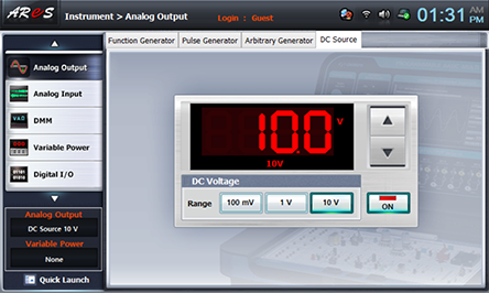
Change the variable resistance R4 for VREF adjustment and turn on all LEDs corresponding to DATA OUTPUT 0~7. Here, adjust the LED corresponding to “0” precisely when it changes from OFF to ON.
- 2Check out the status of Date Output LED when the input DC voltage is set up as table 16-1, and record H when ON and L when OFF in the relevant column of table 16-1. Never change R4 here.
- 3Click at DC source screen to cut of DC power applied to analog input.
Experiment Result Report
1. Experiment Result Table
2. Review and Explanation
1) Analyze items below with the output result in table 16-1.
How is the voltage per 1bit expressed?
Express the output bit when applying analog input 5V, and how is the output voltage expressed?
Output Bit :
Output Voltage :


