PART5Semiconductor
Experiment 3 :NPN Transistor
Theory
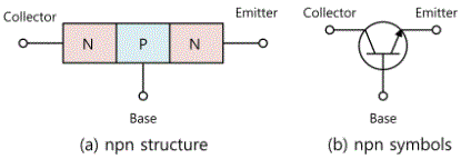
A transistor is made by nearing two semiconductor junctions. Npn transistor is composed of two n materials and a p material, as in Fig. 5-7(a). One area of n material is called collector, and another area is called emitter, and the p area in the middle is called base. In Fig. 5-7 (b), direction of the arrow in the emitter terminal changes by the transistor being npn type or pnp type. As diodes, the front part of the arrow means the direction of the current between emitter and base.
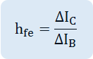
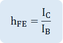
When the emitter becomes a common terminal between the input and the output, it is called a common emitter(CE) structure, and the collector becomes output terminal and the base becomes input terminal. CE Forward current gain is the most important characteristic of the transistor and it is expressed as β or hFE. Here, DC CE forward current gain is expressed as hFE and defined as below.
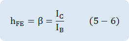
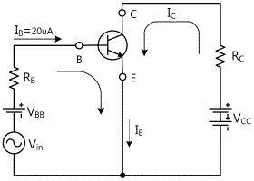
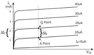
Fig. 5-8 shows the circuit that the base-emitter junction is forward biased, and base-collector junction is reverse biased in CE structure. The characteristic curve of the CE circuit of Fig. 5-7 is in Fig. 5-9.
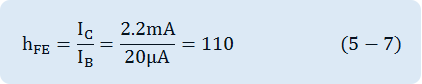
The calculation of hFE for Q point condition of IB=20μA and IC=2.2mA is as below.
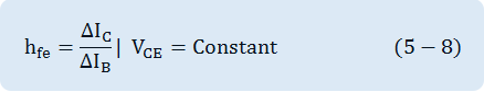
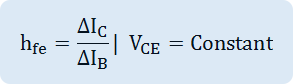
Along with hFE, AC current gain for CE circiuit is used often, and it is defined as below.
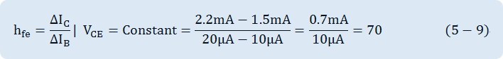
In the transistor of Fig. 5-9, the AC current gain between Q point and A point is calculated as below.
AC current gain hfe is greatly different from DC current gain hFE. In CE circuit, the current gain hfeis bigger to the AC signal. Also, this indicates the important voltage gain. Receiving a small signal and converting it to the big signal of same form is the most useful characteristic of the tran
sistor. This process is called amplification.
According to Kirchhoff’s law of current, the current of transistor can be easily expressed as below.
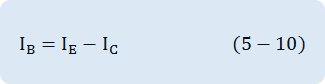
The base current is smaller than that of emitter and that of collector, and is same as the difference between the two. In most calculations, it is ok to consider the emitter current and the collector current as same.
Experiment Process
tab1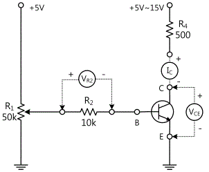
Experiment 5-3.1
NPN Transistor Characteristic Measurement
(In Circuit-3 of M-05, compose a circuit as in Fig. 5-10.)
Measuring (IC) Flowing between R2 and Collector
1.Connection(Circuit-3 of M-05, Fig. 5-10)
1.Power Connection
Connect between V1 terminal of Variable Power on M04 board and VCE 5V~15V 3a(+) terminal of Circuit-3 with red line, and between com terminal and 3b(-) terminal with black line.
2.Measuring Instrument Connection
Ammeter Connection
Measure by using the current measurement function of separate Digital Multimeter.
Measuring the current (Ic) between R2 and collector: Connect the red line of Digital Multimeter to 3e terminal of Circuit-3 and the black line to 3f terminal.
Voltmeter Connection
Measuring the voltage of resistance R4’s both ends: Connect between 3i terminal of R4 and High terminal of Multimeter on the front panel with red line, and between 3j terminal and Low terminal with black line.
2.Wiring Diagram
flash
3.Measurement
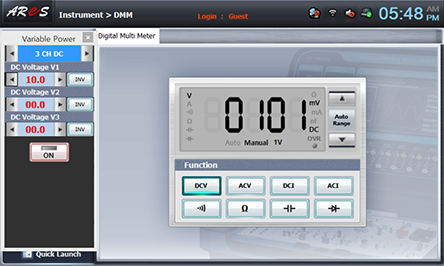
- 1Choose dmm at the left menu of Touch LCD panel and click .
- 2Choose dmm at the bottom of Touch LCD panel and click Variable Power, then 3 CH DC screen appears.
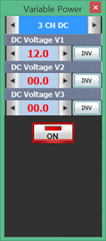
Choose and click at the right of 00.0V to set up the input voltage as DC 10.0V and adjust the voltage value(voltage of R4’s both ends) indicated at Digital Multimeter as Variable Resistance R1 to make it 100mV, then record the current value of separate Digital Multimeter in table 5-5.
Execute the Variable Resistance R1 adjustment and measure by 100mV interval till 800mV.
Variable Resistance R1 is impressed with 5V, so adjust R1 to make IB as 10μA. IB is the base current and calculated by the formula below.
IB=VR2/R2
Therefore, if IB=10μA, VR2=R2×IB=10×103×10×10-6. Therefore, if the voltage of R2’s both ends is 100mV, IB is 10μA. When IB=20μA, estimate by 200mV, and if IB=80μA, estimate by 800mV for IC.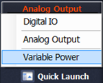
- 3After the measurement, click to cut off the output
Measuring (IC) Flowing between R3 and Collector
1.Connection(Circuit-3 of M-05, Fig. 5-10)
1.Power Connection is same as [Measuring (IC) Flowing between R2 and Collector]>Connection.
2.Measuring Instrument Connection
Ammeter Connection
Measure by using the current measurement function of separate Digital Multimeter.
Measuring the current (IC) between R3 and collector: Connect the red line of Digital Multimeter to 3g terminal of Circuit-3 and the black line to 3n terminal.
Voltmeter Connection
<Voltmeter Connection> is same as [Measuring (IC) Flowing between R2 and Collector]>Connection.
2.Wiring Diagram
flash
3.Measurement
- 1It is same as [Measuring (IC) Flowing between R2 and Collector]>Measurement and record the measured value in the relevant column of table 5-5.
- 2After the measurement, click to cut off the output.
4.Calculation
1. Draw a graph in Graph 5-3 using values of table 5-5, check out the collector current (IC) flowing to R2, R3 when IB is 40μA and calculate the current amplification factor.(when VCE =10V)
Experiment 5-3.2
NPN Transistor Characteristic Measurement
(In Circuit-3 of M-05, compose a circuit as in Fig. 5-10.)
Changing the Base Current IB as 40, 60, 80μA
and Measuring the Collector Current between R2 and Collector for each VCE
1.Connection(Circuit-3 of M-05, Fig. 5-10)
1.Power Connection
Connect between V1 terminal of Variable Power on M04 board and VCE 5V~15V 3a(+) terminal of Circuit-e with red line, and between com terminal and 3b(-) terminal with black line.
2.Measuring Instrument Connection
Ammeter Connection
Measure by using the current measurement function of separate Digital Multimeter.
Measuring the current (IC) between R2 and collector: Connect the red line of Digital Multimeter to 3e terminal of Circuit-3 and the black line to 3f terminal.
Voltmeter Connection
Measuring the voltage of resistance R4’s both ends: Connect between 3i terminal of R4 and High terminal of Multimeter on the front panel with red line, and between 3j terminal and Low terminal with black line.
2.Wiring Diagram
flash
3.Measurement
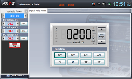
- 1Choose dmm at the left menu of Touch LCD panel and click . Choose quick launch at the bottom of Touch LCD panel and click Variable Power, then 3 CH DC screen appears.
Choose and click at the right of 00.0V to set up the input voltage as DC 4.0V and adjust the voltage value(voltage of R4’s both ends) indicated at Digital Multimeter as Variable Resistance R1 to make it 200mV, then record the current value of separate Digital Multimeter in table 5-6.
Click Variable Power and click at the right of 3 CH DC to adjust it to VCE voltage of table 5-6 and record the measured value of current (IC) of separate Digital Multimeter in table 5-6.
If the voltage of R4’s both ends is out of 200mV(400mV, 600mV, 800mV), execute Variable Resistance R1 Adjustment, make it fit to the setup voltage, measure the current (IC) flowing between R2 and Collector and record it.
- 2After the measurement, click to cut off the output.
Changing the Base Current (IB) as 40, 60, 80μA
and Measuring the Collector Current between R3 and Collector for each VCE
1.Connection(Circuit-3 of M-05, Fig. 5-9)
1.Power Connection is same as [Changing the Base Current (IB) as 40, 60, 80μA and Measuring the Collector Current between R2 and Collector for each VCE]
2.Measuring Instrument Connection
Ammeter Connection
Measure by using the current measurement function of separate Digital Multimeter.
Measuring the current (IC) between R3 and collector: Connect the red line of Digital Multimeter to 3g terminal of Circuit-3 and the black line to 3h terminal.
Voltmeter Connection
<Voltmeter Connection> is same as [Changing the Base Current (IB) as 40, 60, 80 μA and Measuring the Collector Current between R2 and Collector for each VCE].
2.Wiring Diagram
flash
3.Measurement
- 1Execute same as [Changing the Base Current IB as 40, 60, 80μA and Measuring the Collector Current between R2 and Collector for each VCE]Measurement>1) process and record it in table 5-6.
- 2After the measurement, click to cut off the output.
4.Calculation
1. Draw a graph in Graph 5-4 using values of table 5-6, draw a straight line between 10V of the voltage between collector- emitter(VCE) and 6mA of the collector current (IC), make the point where the base current (IB) is 40uA as Q point and calculate the current amplification factor (hFE) which is the DC current gain for Q point condition.
2. Draw a vertical line to Q point and make the point where the base current (IB) is 20uA as A point to calculate ΔIB, ΔIC and calculate AC current gain.
Experiment Result Report
1. Experiment Result Table
2. Review and Explanation
1) Draw a graph in Graph 5-3 using values of table 5-5, check out the collector current (IC) flowing to R2, R3 when IB is 40μA and calculate the current amplification factor. (when VCE=10V)
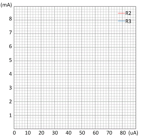 Graph 5-3
2) Draw a graph in Graph 5-4 using values of table 5-6, draw a straight line between 10V of the voltage between collector-emitter(VCE) and 6mA of the collector current (IC), make the point where the base current(IB) is 40uA as Q point and calculate the current amplification factor(hFE) which is the DC current gain for Q point condition.
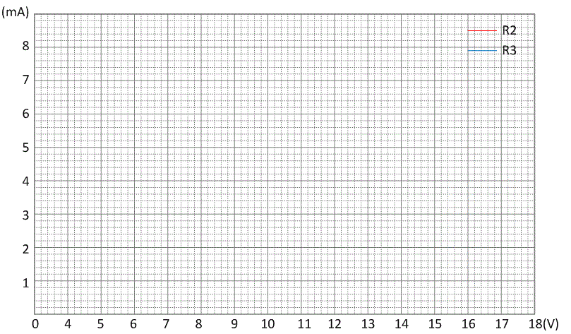 Graph 5-4
3) Draw a vertical line to Q point and make the point where the base current(IB) is 20uA as A point to calculate ∆IB, ∆IC and calculate AC current gain.