PART16Signal Converter
Experiment 2 :Digital to Analog Converter
Theory
DAC Using Weighed Resistance
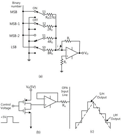
Fig.16-8(a) is one way to earn analog voltage which is proportional to binary number of 4 bit, adding in binary way the current flowing through the weighted resistance R0, 2R0, 4R0, 8R0 with the adder. For example, when the binary number is 1101(13(10)), in the fig., only the switch S1 is off and earthed(in case of MOS switch, it is OFF by making the gate voltage LOW) and the rests are turned ON and connected to the standard voltage VR. Therefore, the output voltage V0 = -RFi becomes as below so the standard voltage should be very precise.

The smaller the input resistance is, the higher the precision should be. Also, the ON resistance of switch should be smaller than 1/2n of the minimum resistance R0.(n: bit number) This is because if the input is generally n bit, the maximum value of the output is as below.

Therefore, for example, if R0=10㏀, and 8 bit, to earn t up to V0= 0 ~ -10V, the biggest input resistance should become 27R0=1.28㏁, RF=R0×10×27/((28-1))=50.196KΩ. Likewise, it is the defect of DAC that the higher the bit is, the bigger resistance is needed. DAC explained later will solve this problem. CMOS inverter in fig.16-8(b) is proper for the switch. Normally, S/H(Sample/Holder) circuit is connected behind DAC. Input digital signal changes parallel at the same time so the output of S/H changes as staircase in fig.16-8(c). To make this as smooth analog signal, LPF is connected behind this. The cutoff frequency of LPF should be lower than clock frequency which operates the switch and higher than the maximum frequency included in the signal.
R-2R Trapezoid DAC
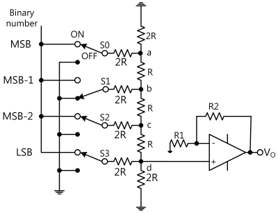
This is the connection of R and 2R as trapezoid and fig.16-9 is about the binary input of 4 bit. Concerning input binary 1101(13(10)), S1 only becomes grounded and the rest is connected to the standard voltage VR and becomes as below.


For instance, when VR = 1V, to make the maximum output as 10V, it should be made as from 1+(R2/R1)/24×15=0 to R2/R1=15.
(1) R-2R trapezoid DAC has double number of resistances compared to weighted R DAC but two resistance values are needed and the characteristic is related to the resistance ratio, not the precision of each resistance, so the precision of resistance ratio should be high
Also, the ON resistance RON of the switch affects more to the MSB part of binary number so the ratio of 2R/RON should be bigger.
(2) The distributed capacity exists between each panel point and the earth. Therefore, as the step voltage occurs at the upper part, delay occurs for delivering to the output and this deters the high speed operation. DAC in fig.16-9 solves this problem.
Experiment Process
1. For the experiment, use Circuit-2 of M-16. And make Circuit-1 of M-16 as below to get the digital output.
2. After connecting between 1e-1f terminal, apply DC 12.75V to 1a-1b terminal.
3. Change R4 of Circuit-1 and turn on all the LEDs corresponding to Data Output 0~7. Here, adjust the LED corresponding to “0” precisely when it changes from OFF to ON.
4. Connect to sockets of Circuit-1 and Circuit-2 using connector cable.
5. In Circuit-2 of M-16, adjust R1 of Circuit-2 so that the voltage between 2c-2d’s both ends becomes DC 12.75V.
6. Record the analog output value when data input(use ADC output of Circuit-1) is applied as in table 16-2 in the relevant column.(determine H, L by the status of LED)
tab1Experiment 16-2.1 Digital to Analog Converter Circuit (Compose as Circuit-2 of M16 and use Circuit-1 as digital input.)
1.Connection
1.Circuit Connection
Vin Input: In Circuit-1 of M16, connect between 1e-1f terminals with yellow line.
Digital Input: Connect between DB0(0)~DB7(7) terminals of Circuit-1 and A8(0)~A1(7) terminals of Circuit-2 with yellow lines matching each other.
2.Power connection is internally connected.
3.Measuring Instrument Conenction
Signal Output Connection
Connect between 1a terminal of Circuit-1 and A+ terminal of Signal Output on the front panel with red line, and between 1b terminal and A- terminal with black line.
Voltmeter Connection
On the Multimeter of front panel, connect between High terminal and 2c terminal of Circuit-2 with red line, and between Low terminal and 2d terminal with black line.
2.Wiring Diagram
3.Measurement
- 1Execute [Analog to Digital Converter Circuit]>3. Measurement>1) process.
- 2In Circuit-2 of M16, make the voltage of Analog Output(2c-2d)’s both ends as DC 10V.
At Touch LCD, choose dmm, click and adjust R2 of Circuit-2 to make DC 10V.
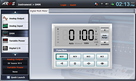
- 3Execute [Analog to Digital Converter Circuit]>3. Measurement>2) Process and record the analog output value when data input(use ADC output of Circuit-1) is applied as in table 16-2 in the relevant column.(determine H, L by the status of LED)
Click quick launch at the left bottom of Touch LCD, choose Analog Output and click of funnction to make DC Source window appear.
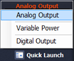

Click at 05.0v of Range and record the value indicated at Digital Multimeter when the output of LED is same as Digital Input (Binary Input) of table 16-2.
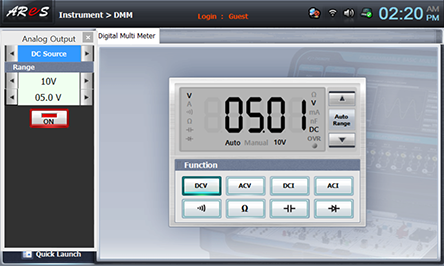
- 4Click at DC source screen to cut of DC power applied to analog input.


