PART14Sequential Logic Circuit
Experiment 4 :Shift Register
Theory
“Shift” means “to change the location, to move” and the operation of register is executed by the input of clock pulse.
Here, let’s investigate the operation status of shift register. Say the 6 bit data 101101 is stored in shift register. Fig.14-14(a) displays this status. If one clock pulse is applied to this status, the 1 in LSB(least significant bit) is thrown out and discarded as in fig.14-14(b) and each bit gets the number that is on 1 bit left.
Here, MSB(most significant bit) gets external data. In the fig., the external data is all 0 so whenever 1bit right shift is executed, “0” enters to MSB. This is one example of right shift.
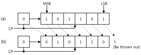
Fig. 14-15(a) is the right shift register composed by using D flip-flop. Here, if the data value currently stored in D flip-flop of each terminal is 1010 and if new external data serial input 11010 is entered to D input, and if the data moves to 1 bit right in trailing edge status of clock pulse(that is, shift pulse), the operation status is displayed in fig.14-15(b).

(a) Shift Register using D Flip-flop
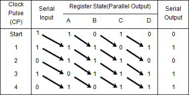
(B) State Table of 4 bit Right Shift Register
With shift register, multiplication and division are possible. That is, in case of one left shift, the result is doubled, and in case of one right shift, the result is divided by 2. For example, if 5 bit binary data value is (10000)2, if it is shifted to the right once, it becomes (1000)2, and if it is shifted to the right again, it becomes (100)2. Here, if the binary data value is changed to decimal number, 5 bit (10000)2 becomes (16)10, and (1000)2 becomes (8)10, and (100)2 becomes (4)10. If 16 is moved 1 bit right, it becomes 16 ÷ 2 = 8, and if it is moved to the right again, it becomes 8 ÷ 2 = 4. As a result, if the number is moved 1 bit to the right, it is divided by 2. And if it is moved 1 bit to the left, it is doubled.
Experiment Process
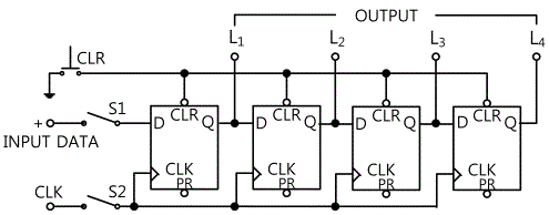
1. In Circuit-4 of M-14, compose a shift register as in fig.14-16.(Connect from Manual Pulse Output to 4a terminal.)
2. When the data is applied as in table 14-5, as the clock is applied, measure each output L1, L2, L3, L4 of the output terminal and record the result in table 14-5. The data input means H when the switch S1 is ON, and L when it is OFF. However, before applying the clock, press CL switch once to clear the data within the shift register.
tab1Experiment 14-4.1 Serial Input/Parallel Output Shift Register Circuit Experiment (Cuircuit-4 of M14)
1.Connection
1.Circuit Connection
In Circuit-2 of M14, connect between 2b terminal and 4a terminal of Circuit-4 with yellow line.
Connect between 4d terminal on LED1(A) of Circuit-4 and (A) terminal on the 7-Segment Display at the center, between 4e terminal of LED2(B) and (B) terminal, between 4f terminal of LED3(C) and (C) terminal, and between 4g terminal of LED4(D) and (D) terminal with yellow lines
2.Power connection is internally connected.
3.Measuring Instrument Connection
Connect BNC cable to Signal Output on front panel, connect red lead wire to 4a(CLK) terminal of Circuit-4 on M14 board.(Connect black lead wire to 3h(GND) of Circuit-3.)
2.Wiring Diagram
flash
3.Measurement
- 1In Circuit-4 of M-14, compose a serial input/parallel output shift register as in fig.14-16.
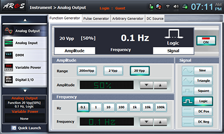
- 2Choose analog output at Touch LCD panel, and click Function Generator.
Set up Amplitude Range as , and Amplitude as amplitude 50% using .
Choose at Frequency to make frequency 0.1hz.
Set up Signal as , and click to output the logic signal 0.1Hz to Circuit-4.
- 3When data is applied as table 14-5 and as the logic pulse is applied, record “1” in table 14-5 when each output of the output terminal LED1(A), LED2(B), LED3(C), LED4(D) are on, and “0” when they are off. The data input means “1” when the switch S1 is ON, and “0” when it is OFF.
Before applying the clock(CLK), press CL(Clear) once to clear the data within the shift register.
- 4Record the hexadecimal numbers displayed at 7-Segment Display in table 14-5.
- 5After the measurement, click at analog output of Touch LCD panel and cut off the logic pulse output to Circuit-4.
Experiment Result Report
1. Experiment Result Table
2. Review and Explanation
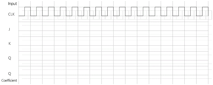
1) Draw a timing chart with the result in table 14-5.