PART12Pulse Circuit
Experiment Purpose
- 1.Investigate characteristics of clipping circuit.
- 2.Investigate characteristics of Schmitt-trigger circuit through experiment.
- 3.Investigate characteristics of bistable multivibrator circuit experiment.
- 4.Investigate characteristics of monostable multivibrator circuit through experiment.
The circuit used to transfer certain parts of wave form, which are higher or lower than certain standard level, is called clipping circuit, limiter or amplitude limiter.
Experiment 1 :Clipping Circuit
Theory
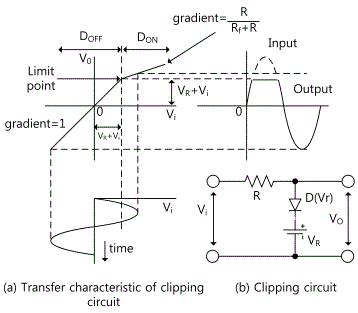
In fig.12-2(b), if partial linear model of the diode is used, the transfer characteristic of fig.12-2(a) can be earned. Compared to the threshold voltage(or block offset) voltage Vr, when the input voltage νi is νi≤Vr+VR, the diode voltage becomes as ν<Vr and the diode is cutoff. Here, the electric current does not flow to the resistance R so the output ν0 becomes ν0=νi. When the input signal is within the range from (-) value to VR+Vr, the transfer characteristic curve becomes a straight line whose gradient is 1. Next, if the input signal νi becomes bigger as νi≥VR+Vr, D is conducted and operated as a battery Vr whose inner resistance is Rf. Here, the output voltage ν0 is as below.

That is, the increment of input △νi decreases, and that of output △ν0 is as below.

You can see that this is the straight line part of the gradient Rf/(Rf + R) to νi > VR + Vr in the transfer curve. The amplitude of input signal in fig.12-2(a) is a much bigger wave form than point of inflexion, so parts of (+) in the amplitude of output signal is cut. This means the cut of the input signal’s (+) maximum value, and if Rf <R, the degree of cut is much bigger so the maximum value of output signal is limited as VR + Vr. Normally, VR ≫ Vr, so VR only can be used as standard voltage.
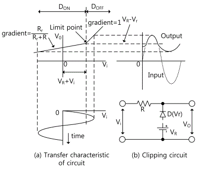
Contrary to the previous case, a diode is connected to the clipping circuit of fig.12-3(b). When partial linear model is applied to the transfer characteristic, the characteristic in fig.12-3(a) can be earned. In this circuit, the linear parts where the input signal is (+) which is bigger than VR - Vr is transferred without attenuation, but the parts lower than (+) voltage are not output. In fig.12-2(1) and fig.12-3(a), the reverse resistance of diode Rr is supposed as Rr≫R. The circuit which cannot satisfy this condition should correct the transfer characteristic. The straight line parts whose gradient is 1 should be substituted for the gradient of Rr/(Rr+R), and in the transfer of diode clipping circuit, Rr≫R. Fig.12-4 shows a generally used diode clipping circuit. To simplify the operation of this circuit, the diode is considered ideal and the inner resistance is ignored. That is, the diode is supposed to operate as an ideal ON-OFF switch.
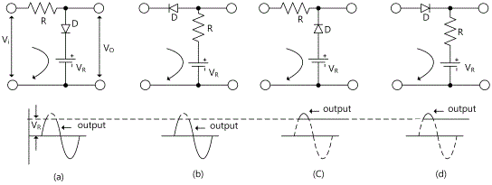
In the circuit of fig.12-4 (a), when the input voltage νi is smaller than the standard voltage VR, D is in cutoff state, that is, the circuit is same as the open circuit, and if the input voltage νi is bigger than VR, the diode is conducted, and actually operated as a short circuit. Therefore, the output V0 is as below.

The case where the input signal is applied as sine wave is indicated in fig.12-4. The clipping wave form of the formula above is the wave form that cuts off the parts over the standard voltage VR from input wave form and is indicated in the output side. Fig.12-4(c) is the circuit in which the polarity of D is inverted. In this circuit, when νi < VR, D is conducted, and when νi > VR, it is cutoff. Therefore, the output ν0 of this case is as below.

As seen in the fig., the output wave form is the shape that the parts below the standard voltage VR is cutoff from the input wave form. Fig.12-4(a) and (c) are called parallel clipping circuits. And fig.12-4(b) and (d) are clipping circuits composed by inputting a diode in series to the transmission line of the signal, so they are called serial clipping circuits.
Slice or Limiter Circuit
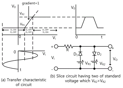
A diode clipping circuit which is composed of double diodes in order to transfer only the signals between two standard voltages VR1 and VR2 is called a slice(limiter) circuit. This circuit can be composed as parallel-serial or serial-parallel connection, and fig.12-5(b) shows the parallel case. The transfer characteristic curve has two points of inflexion of ν0 = νi = VR1 and ν0 = νi = VR2, and has characteristics as below. Here, VR2 > VR1 ≫ Vr and Rf ≪ R. When the input voltage νi is as below, the states of output voltage and diode are as below.
| Input Signal Vi | Output Signal V0 | State of Diode |
|---|---|---|
| Vi ≤ VR1 VR1 ≤ Vi ≤ VR2 Vi ≥ VR2 |
V0 = VR1 V0 = Vi V0 = VR2 |
D1 : ON,D2 : OFF D1 : OFF,D2 : OFF D1 : OFF,D2 : ON |
This slice circuit is used to earn a square wave from a sine wave signal, and to get a symmetrical square wave, the absolute values of VR1 and VR2 are same but their polarities are opposite. In this condition, the transfer characteristic curve passes the origin and the input wave form cuts as its upper and lower parts becomes symmetry. When the amplitude of input signal is much bigger than the difference between the standard voltage VR1 and VR2, the input signal becomes a square wave.
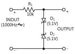
And if zener diode is connected in series reversely as in fig.12-6(a), it is operated as a clipper which has same characteristic as fig.12-6(b).
If the diode has same characteristic, a amplification limiter which is symmetrical can be earned. If the breakdown voltage of zener diode is VZ and the cutoff voltage is Vr, the transfer characteristic of fig.12-6(b) is earned.
Experiment Process
1. In Circuit-1 of M12, compose a circuit as in fig.12-7 and make the input as sine-wave 1000Hz.
2. As given in table 12-1, measure the output voltage between 1f-1g terminals for each input voltage and record the result in the relevant column of table 12-1. Check out the output wave form and compare it with the input wave form.
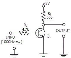
3. In Circuit-1 of M12, compose a circuit as in fig.12-8 and make the input as sine-wave 1000Hz.
4. As given in table 12-2, measure the output voltage between 1l-1m terminals for each input voltage and record the result in the relevant column of table 12-2. Check out the output wave form and compare it with the input wave form.
tab1Experiment 12-1.1 Clipping Circuit Experiment (In Circuit-1 of M12, compose circuits as in fig.12-7, 8.)
Diode Clipping Circuit, Fig.12-7 of Circuit-1
1.Connection
1.Power connection is internally connected.
2.Measuring Instrument Connection
Function Generator Connection
Plug in BNC cable to BNC terminal of Signal Output on front panel and connect red line to 1a terminal of Circuit-1, and black line to 1b terminal.
Oscilloscope and Voltmeter Connection
Input Voltage Measurement Connection: Connect between 1a terminal of Circuit-1 and A+ terminal of Signal Input CH A on the front panel of Multimeter with red line, and between 1b terminal and A- terminal with black line.
Output Voltage Measurement Connection: Connect between 1f terminal of Circuit-1 and B+ terminal of Signal Input CH B on the front panel of Multimeter with red line, and between 1g terminal and B- terminal with black line.
2.Wiring Diagram
3.Measurement
- 1In Circuit-1 of M12, compose a circuit as in fig.12-7 and make the input as sine-wave 1000Hz.
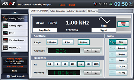
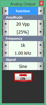
Choose analog output at Touch LCD panel, set up Amplitude Range as , and Amplitude as amplitude 25%. Choose at Frequency to make 1khz. Set up Signal as , and click to send the output to Circuit-1.
In table 12-1, when the input voltage is 5Vpp, 10Vpp, 15Vpp, 20Vpp, 25% of becomes 5Vpp so measure by setting up the Amplitude as 25%, 50%, 75%, 100%.
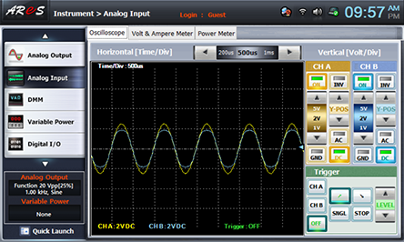
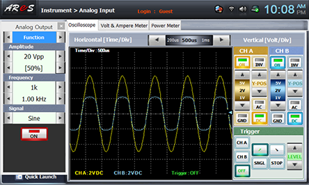
Choose analog input at front panel and draw the wave form in oscilloscope screen in the relevant column of table 12-1.
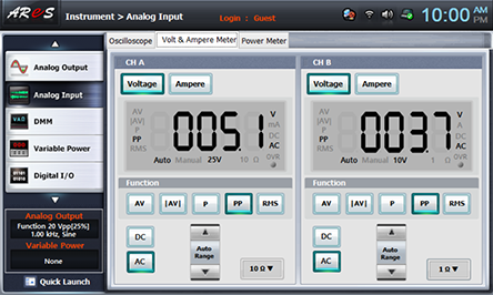
Choose Volt & Ampere Meter tab and click , , at CH A, CH B and record the indicated output voltage in the relevant column of table 12-1.
- 2Measure the output wave form and voltage in cases of 10Vpp, 15Vpp, 20Vpp.
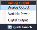
Choose quick launch on the left bottom of the screen, click Analog Output and click of Amplitude 25% to change the amplitude as 50%, 75%, 100%. Record the indicated output wave form in the relevant column of table 12-1.
10Vpp :
10Vpp :

15Vpp :
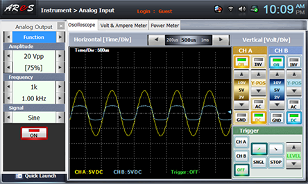
15Vpp :
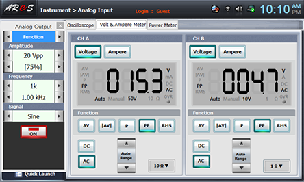
20Vpp :

20Vpp :

- 3After the measurement, click at quick launch screen and cut off the output.
Transistor Clipping Circuit, Fig.12-8 of Circuit-1
1.Connection
1.Power connection is internally connected.
2.Measuring Instrument Connection
Oscilloscope and Voltmeter Connection
Input Voltage Measurement Connection: Connect between 1h terminal of Circuit-1 and A+ terminal of Signal Input CH A on the front panel of Multimeter with red line, and between 1i terminal and A- terminal with black line.
Output Voltage Measurement Connection: Connect between 1l terminal of Circuit-1 and B+ terminal of Signal Input CH B on the front panel of Multimeter with red line, and between 1m terminal and B- terminal with black line.
2.Wiring Diagram
3.Measurement
- 1Execute [Diode Clipping Circuit, Fig.12-7 of Circuit-1]>3. Measurement and record the input/output waveform and output voltage in the relevant column of table 12-2.
5Vpp :

5Vpp :

10Vpp :

10Vpp :

15Vpp :

15Vpp :
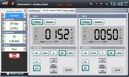
20Vpp :

20Vpp :

- 2After the measurement, click at quick launch screen and cut off the output.


